Using nano-helical polymers to improve optoelectronic chips
Findings will be useful in next-generation optoelectronics, polarization imaging and cryptographic communication.
Findings will be useful in next-generation optoelectronics, polarization imaging and cryptographic communication.
Collaborative research between Seoul National University and the University of Michigan recently published in Nature describes next-generation optoelectronic chips used for a range of applications from automobiles and aviation to information processing and machine vision.
Optoelectronics is a branch of electronics that deals with the use of light to control the flow of electrical current.
“Helical photons offer a realistic pathway for quantum computing and spintronic devices, however, the current chips can measure only the intensity of the incident light rather than its helicity, which remains a key barrier in implementation of these powerful technologies,” said Nicholas A. Kotov, Joseph B. and Florence V. Cejka Professor of Chemical Engineering, and Irving Langmuir Distinguished Professor of Chemical Sciences and Engineering at University of Michigan.
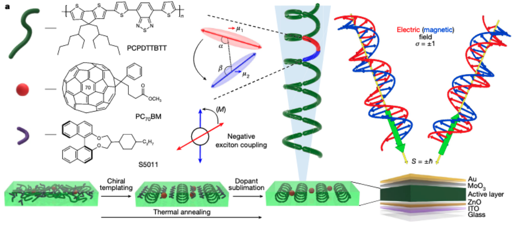
Interactions of light with a chiral nanomaterial, spiraled like DNA, can theoretically be used for making optoelectronic chips, but sensitivity and accuracy of polarization detection by traditional chiral materials is low.
The team of scientists found an efficient method to fabricate highly homogeneous layers of polymers with supramolecular helical ordering that display the chirality at molecular and nanometer scales while providing intense light-matter interactions. This eliminates the need for elaborate optical designs and labor-intensive fabrication that were previously required.
“Helicity of the nanoscale polymer coils imparted by the small chiral molecules developed at Seoul National University, is a powerful tool for the polymeric materials suitable for direct integration with optical chips.”
Nicholas Kotov
Joseph B. and Florence V. Cejka Professor of Chemical Engineering
“Helicity of the nanoscale polymer coils imparted by the small chiral molecules developed at Seoul National University, is a powerful tool for the polymeric materials suitable for direct integration with optical chips,” Kotov said. “Nano-helical polymers make possible simple technology for manufacturing of a new generation of chiral photonic devices utilizing helicity of light for optical communication and quantum computing devices operating at room temperature.”
The chirality of helical photons is a convenient property to differentiate them from one another. However, making chips that can sense the helicity is difficult due to problems with homogeneity and sensitivity for light polarization.
The chiral polymer described in this work makes it possible, demonstrating optoelectronic chips capable of rapid sensing of helical photons.

“A universal strategy has been successfully devised for manufacturing a photoactive layer made of helical polymers, which possesses an inherent ability to detect the spin angular momentum of photons,” said Joon Hak Oh, Professor of Chemical and Biological Engineering at Seoul National University. “This pioneering development is expected to drive significant advancements in the commercialization of chiral optoelectronic chips, which have thus far been limited to unit device levels.”
This work builds upon the foundation of extensive studies of chiral nanostructures taking place around the world, including research completed as part of the CHIPS and Science Act to support U.S. leadership in semiconductor manufacturing.
This progress results in extraordinarily high sensitivity to helicity of light, enabling real-time control of the spin angular momentum in light detection and imaging over a large area which will be useful in next-generation optoelectronics, like polarization imaging and crypto-communication.
This work was supported by the Samsung Research Funding Center of Samsung Electronics, the National Research Foundation of Korea and Nano Material Technology Development Program funded through the National Research Foundation of Korea by the Ministry of Science and ICT. The Institute of Engineering Research at Seoul National University provided research facilities for this work. The work from the University of Michigan was supported by Vannevar Bush Fellowship from the Office of Naval Research.